NAND Flash (NAND Flash)
NAND Flash 协议分析设置。
更多应用、连接与量测说明请见 Protocol Solution — NAND Flash。
Supported Models
LA3000/LA4000
LA4000 僅於 B 系列支援 此功能需要额外购买 option 的功能。
BusFinder
BF6000 僅於 B 系列支援, BF7000 全系列都支援 此功能需要额外购买 option 的功能。
Settings
- 设定:
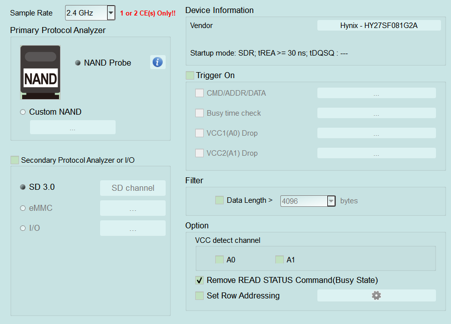
- Sample Rate: 选择采样率。若要开启 Secondary Protocol Analyzer(SD 3.0/eMMC),采样率须设为 1 GHz 以下。Default 为 2.4 GHz。
- Primary Protocol Analyzer: 选择 NAND Probe,或 Custom NAND 自定义通道/接线。
- Secondary Protocol Analyzer or I/O: 以剩余脚位同时开启 SD 3.0、eMMC 或 I/O 分析。
- Vendor: 选择 NAND 厂牌/型号;若无合适项目可选 Custom 自定义 Command Set。画面会显示 Startup mode、tREA、tDQSQ 等状态。Default 显示约 Startup mode: SDR; tREA >= 30 ns。
- Filter: 勾选后 Data Length > 栏位启用(Enable)。Default 为未勾选。
- Option:
- Invert RE# (W/R#)/Invert DQS: DDR 模式下若接到反向的 RE/DQS 差分信号线,勾选以告知软件。Default 为未勾选。
- Don't care R/B: 忽略 R/B,可不接 R/B 信号线。Default 为未勾选。
- Single R/B#: Multi-CE 时,勾选以 Read Status Ready 显示 Busy time;未勾选则以 R/B 判断。Default 为未勾选。
- Remove READ STATUS Command (Busy State): 移除重复的 Not Ready Polling Read Status。Default 为勾选。
- Set Row Addressing: 将 Row Address 细分为 Page/Word Line/Plane/Block/LUN 等;勾选后 Set 按钮栏位启用(Enable),开启 Set Row Addressing 弹出窗口(见下方说明)。默认值来自 NAND Command Set。Default 为未勾选。
- 触发设定:
- Trigger on: 勾选后可设定 CMD/ADDR/DATA、Busy time check、VCC1(A0)/VCC2(A1) Drop;子项勾选后齿轮栏位启用(Enable)。弹出窗口 Default: CMD XXh、Row XXXXXXh;Busy 约 250 ms。Default 为 Trigger on 与各子项未勾选。
- VCC1(A0) Drop/VCC2(A1) Drop: 电压下降触发;开启 Voltage Range Settings(说明见 Settings — Voltage Range Settings)。常见范围约 VDD1 2.70~3.60 V、VDD2 1.70~1.95 V。
- Trigger on: 勾选后可设定 CMD/ADDR/DATA、Busy time check、VCC1(A0)/VCC2(A1) Drop;子项勾选后齿轮栏位启用(Enable)。弹出窗口 Default: CMD XXh、Row XXXXXXh;Busy 约 250 ms。Default 为 Trigger on 与各子项未勾选。
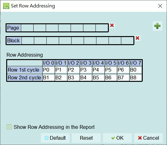
在 Option → Set Row Addressing 勾选后按 Set 开启此窗口: 可定义 Page/Block(或 Word Line/Plane/LUN 等)位宽,并在 Row Addressing 表中对应各 cycle 的 I/O 0~7(例如 P0P6、B0B8);可勾选 Show Row Addressing in the Report 于报告显示,并以 Default/Reset 还原或清除。