NAND Flash (NAND Flash)
NAND Flash Protocol Analyzer settings.
For application notes, probe connection, and measurement details, see Protocol Solution — NAND Flash.
Supported Models
LA3000/LA4000
LA4000 is supported only on B series. This feature requires purchasing an additional option.
BusFinder
BF6000 is supported only on B series, all BF7000 models are supported. This feature requires purchasing an additional option.
Settings
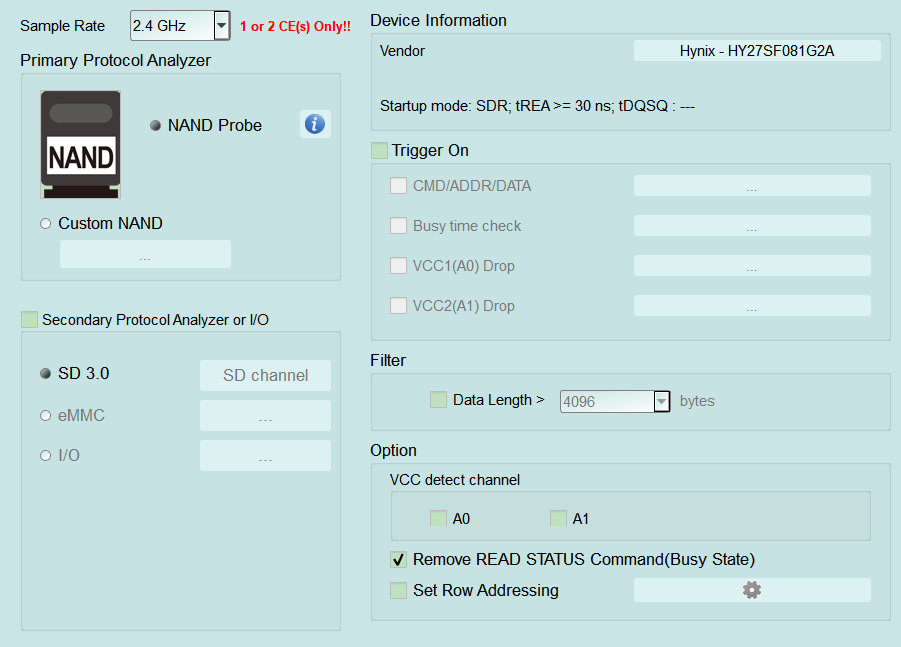
- Settings:
- Sample Rate: Select the sample rate. If Secondary PA (SD 3.0 / eMMC) is enabled, use 1 GHz or below. Default: 2.4 GHz.
- Primary Protocol Analyzer: Choose NAND Probe or Custom NAND wiring.
- Secondary Protocol Analyzer or I/O: Run SD 3.0, eMMC, or I/O on remaining pins.
- Vendor: Select NAND vendor/part, or Custom command set (edit samples in the working directory, then Refresh). Status shows Startup mode, tREA, tDQSQ, etc. Default status about Startup mode: SDR; tREA >= 30 ns.
- Filter: When checked, Data Length > is enabled (Enable) — drop data beyond the set byte length per Data Frame. Default: cleared.
- Option:
- Invert RE# (W/R#) / Invert DQS: When probing inverted differential RE/DQS in DDR mode. Default: cleared.
- Don't care R/B: Ignore R/B (R/B wiring optional). May disable (Disable) Busy-time items. Default: cleared.
- Single R/B#: In Multi-CE, use Read Status Ready for Busy time when checked; otherwise use R/B. Default: cleared.
- Remove READ STATUS Command (Busy State): Remove repeated Not Ready Polling Read Status. Default: checked.
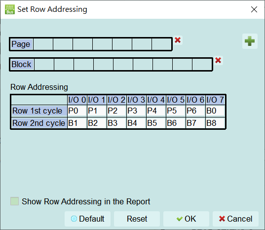
- Set Row Addressing: Split Row Address into Page / Word Line / Plane / Block / LUN, etc.; Set button enabled (Enable) when checked, opening the Set Row Addressing dialog (see below). Defaults come from the NAND Command Set. Default: cleared.
- Trigger settings:
- Trigger on: When checked, configure CMD/ADDR/DATA, Busy time check, VCC1(A0)/VCC2(A1) Drop; gears are enabled (Enable) per child and first check often opens a dialog. Dialog Default: CMD XXh, Row XXXXXXh, Data XXh/XXXXh; Busy about 250 ms. Default: Trigger on and children cleared.
- VCC1(A0) Drop / VCC2(A1) Drop: Voltage-drop trigger; open Voltage Range Settings (see Settings — Voltage Range Settings). Typical VDD1 about 2.70–3.60 V, VDD2 about 1.70–1.95 V.
- Trigger on: When checked, configure CMD/ADDR/DATA, Busy time check, VCC1(A0)/VCC2(A1) Drop; gears are enabled (Enable) per child and first check often opens a dialog. Dialog Default: CMD XXh, Row XXXXXXh, Data XXh/XXXXh; Busy about 250 ms. Default: Trigger on and children cleared.
Open this dialog from Option → Set Row Addressing (check the option, then click Set). Define bit widths for Page / Block (or Word Line / Plane / LUN, etc.) and map them onto I/O 0–7 for each cycle in the Row Addressing table (e.g. P0–P6, B0–B8). Optionally enable Show Row Addressing in the Report. Use Default / Reset to restore or clear.