SWD (Serial Wire Debug)
SWD (Serial Wire Debug) is an ARM test protocol on SWDIO and SWDCLK. It provides access to the CoreSight™ Debug Access Port and can replace JTAG when pin count is limited.
Wrong Bit Order or AP type yields incorrect register interpretation. For channel-prefix differences, see Settings.
Decode Settings
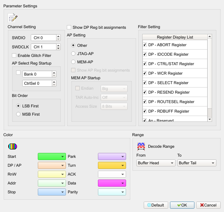
- SWDIO: I/O signal channel.
- SWDCLK: Clock signal channel.
- Select Reg startup: When the AP Select Register initial value is unknown, the LA shows addresses instead of register names; set Bank and Ctrl/Select manually. Field enabled (Enable) when checked. Default: cleared; Bank/CtrlSel Default: 0/0.
- Bit Order: LSB or MSB. Default: LSB First.
- Show DP Reg bit assignments: Show DP register field meanings. Field enabled (Enable) when checked. Default: cleared.
- AP Setting: Decode AP registers as MEM-AP, JTAG-AP, or Other. Other shows only Bank X Register X. Default: Other.
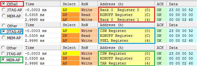
- Show AP Reg bit assignments: Show AP register field meanings; field enabled (Enable) when MEM-AP or JTAG-AP is selected. Default: cleared.
- MEM-AP startup: When MEM-AP is selected, initialize MEM-AP contents; matching addresses update during capture. Checking Endian enables (Enable) data with read/write addresses. Default Endian: cleared; Endian type index 0 (Big); TAR Auto-Inc index 0 (Off); Access Size index 0 (8 Bits).

- Filter Setting: Filter registers you do not need to observe. Default: registers checked (shown).
- Enable Glitch Filter: Enable glitch filtering. Field enabled (Enable) when checked. Default: cleared.
Result