SPI NAND
The SPI NAND Flash Memory series uses the SPI/QPI protocol. SPI NAND bus analysis shows command and I/O bus information while viewing signals, reducing time spent on SPI waveform analysis.
Incorrect Vendor, timing, or read mode versus the IC can cause decode errors. For channel-prefix differences, see Settings.
Decode Settings
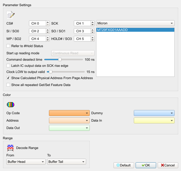
- CS#: Chip Select.
- SCLK: Clock.
- SIO0 – SIO3: Data pins (including WP/HOLD#).
- Vendor/IC: Select vendor and IC; switching may update default timing. Default is Micron (first IC in the list).
- Start up reading mode: Initial read state (Continuous Read/Buffer Read). Field enabled (Enable) only when the IC supports continuous read. Default is Continuous Read.
- Command deselect time: Hold time to treat CS# as inactive (tSHSL). Default is 50 ns (may be overwritten by the IC table after selection).
- Clock LOW to output valid: Positions actual data (tCLQV). Field enabled (Enable) when Latch on rise is cleared. Default is 15 ns (may be overwritten by the IC table).
- Refer to #Hold Status: Decode using the #Hold pin state. Field enabled (Enable) when checked. Default is cleared.
- Latch IC output data on SCK rise edge: Latch and decode IC output on the SCK rising edge. Field enabled (Enable) when checked; tCLQV is field disabled (Disable). Default is cleared.
- Show Calculated Physical Address From Page Address: Show the full physical address computed from the page address. Field enabled (Enable) when checked. Default is checked.
- Show all repeated Get/Set Feature Data: Show all repeated Get/Set Feature data. Field enabled (Enable) when checked. Default is cleared.
Result
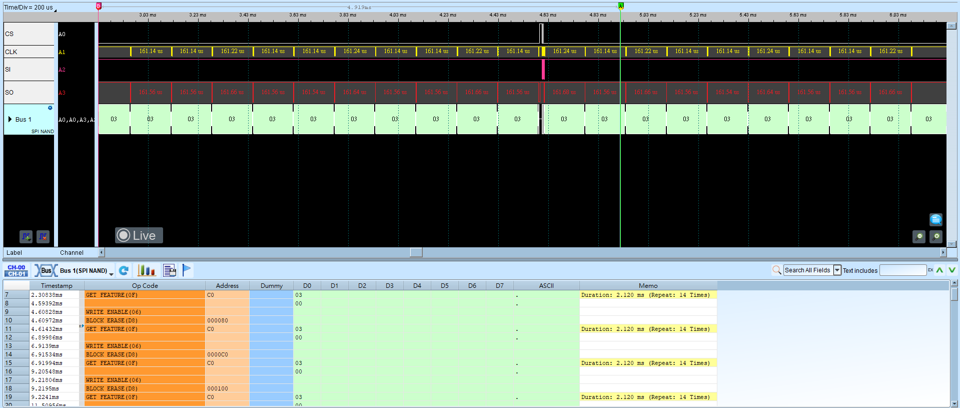
When Op Code = Get Feature (0F), the report removes repeated values and marks Duration time.